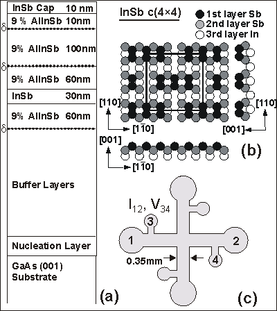
 Figure 1: Schematics of the sample
(a)Typical epitaxial layer growth sequence for modulation-doped samples. (b) Atomic model of InSb c(4x4) surface reconstruction showing top and side views. (c) Hall-bar pattern used to investigate the anisotropic transport.
Figure 1: Schematics of the sample
(a)Typical epitaxial layer growth sequence for modulation-doped samples. (b) Atomic model of InSb c(4x4) surface reconstruction showing top and side views. (c) Hall-bar pattern used to investigate the anisotropic transport.
In this study, five quantum well samples and one sample with a bulk InSb layer were investigated. There were slight variations in nucleation and buffer layers for the different samples.
As shown in the Fig. 1(a), two d-doped layers were placed on either side of the 30nm well, 60nm into the Al0.09In0.91Sb layers. The third dopant layer compensates for surface states.
Figure 1(b) shows the reconstruction of the surface during growth of the quantum wells and barrier, as determined by RHEED. Note the anisotropy in the [ 0 0 1] surface: continuous channels extend in the [ 1-1 0] direction but not in the [ 1 1 0] direction. This anisotropy gives rise to anisotropy in diffusion lengths of ad-atoms on the surface and will affect growth of the material.
The Hall bar sample shown in Fig. 1(c) allows measurement of m in the [ 1 1 0] and [ 1-1 0] directions. This pattern was used to define a mesa on the sample. Contacts were made to the sample by evaporating In through a mask with circular contact openings. Ohmic contacts were achieved by annealing a 230°C for 5 minutes. Gold wires were bonded to these contacts with In solder. Statistics of defects on the growth surface were determined in the center of the cross.