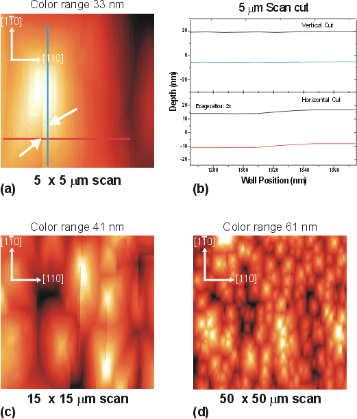
Figure 2 - S476
10 x [25 nm InSb 120 nm 9% AlInSb]
The three figures: (a), (c) and (d) are AFM images of the same sample at different latteral resolutions.
Figure (a) is 5 mm2 scan showing a detailed image of a hillock.
The graduating color rings about the hillock are steps of one atomic layer (~10 Å) which form the basis of a
screw dislocation. The red and blue lines as well as the arrows in the figure indicate the location of cross-sectional
plot in figure (b). A simulated well profile is also shown with the horizontal axis exagerated by a factor of 2
to clarify the compression of the well thickness due to the step in the hillock.10 x [25 nm InSb 120 nm 9% AlInSb]
Using the 15 and 50mm2 scans (figures (c) and (d) respectively) the hillock and O.A.S. density and size were calculated for comparison to the optical and crystalline properties of the sample.
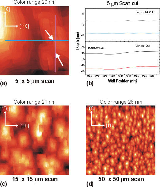
Figure 3 - S477
10 x [25 nm InSb 50 nm 9% AlInSb]
The three figures: (a), (c) and (d) are AFM images of the same sample at different latteral resolutions.
Figure (a) is 5 mm2 scan showing a detailed image of a hillock.
The graduating color rings about the hillock are steps of one atomic layer (~10 Å) which form the basis of a
screw dislocation. The red and blue lines as well as the arrows in the figure indicate the location of cross-sectional
plot in figure (b). A simulated well profile is also shown with the horizontal axis exagerated by a factor of 2
to clarify the compression of the well thickness due to the step in the hillock.10 x [25 nm InSb 50 nm 9% AlInSb]
Using the 15 and 50mm2 scans (figures (c) and (d) respectively) the hillock and O.A.S. density and size were calculated for comparison to the optical and crystalline properties of the sample.
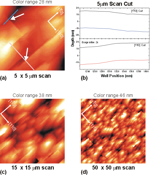
Figure 4 - S595
25 x [25 nm InSb 50 nm 9% AlInSb]
The three figures: (a), (c) and (d) are AFM images of the same sample at different latteral resolutions.
Figure (a) is 5 mm2 scan showing a detailed image of a hillock.
The graduating color rings about the hillock are steps of one atomic layer (~10 Å) which form the basis of a
screw dislocation. The red and blue lines as well as the arrows in the figure indicate the location of cross-sectional
plot in figure (b). A simulated well profile is also shown with the horizontal axis exagerated by a factor of 2
to clarify the compression of the well thickness due to the step in the hillock.25 x [25 nm InSb 50 nm 9% AlInSb]
Using the 15 and 50mm2 scans (figures (c) and (d) respectively) the hillock and O.A.S. density and size were calculated for comparison to the optical and crystalline properties of the sample.